
Key Takeaways
- HDI boards use laser-drilled microvias and sequential lamination to support compact, high-pin-count components.
- Standard boards rely on through-holes and wider traces, which limit routing density.
- Choosing an HDI PCB manufacturer affects signal integrity, thermal paths, and inspection requirements.
Introduction
Engineers working with PCB manufacturing in Singapore often face a practical decision. A standard board may meet electrical requirements, yet physical constraints can block component placement or signal routing. Compact devices such as wearables, smartphones, and control modules demand tighter layouts and shorter electrical paths. High-Density Interconnect technology addresses these constraints through controlled fabrication steps and specialised equipment. The difference between standard production and HDI capability appears in specific technical processes, not marketing labels. The following seven factors outline what separates conventional PCB builds from true HDI manufacturing.
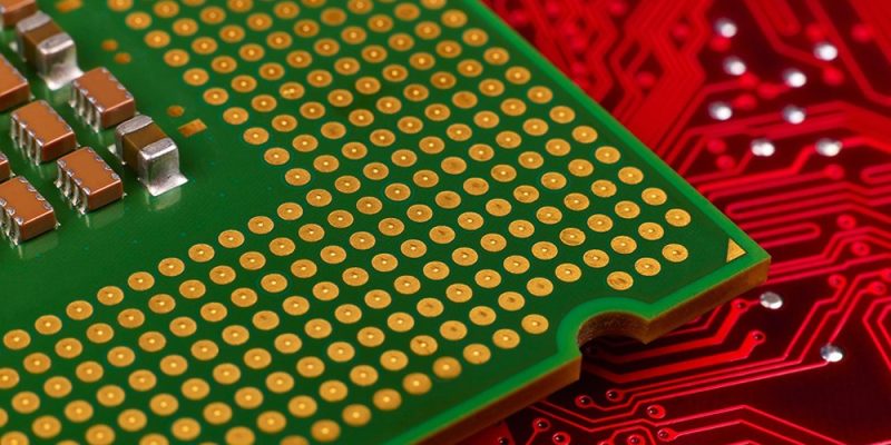
1. Microvias Replace Traditional Through-Holes
Standard boards use mechanically drilled through-holes that pass from the top layer to the bottom layer. These holes consume routing space on every layer they cross. HDI production replaces many of these with laser-drilled microvias. Microvias connect only selected layers, usually outer to inner layers, and measure significantly smaller than traditional vias. This reduction in size frees surface area for fine-pitch components and dense routing. An HDI PCB manufacturer must maintain tight drilling tolerances and controlled depth to ensure reliable connections.
2. Sequential Lamination Builds Layer Complexity
Conventional multilayer boards typically complete lamination in a single pressing cycle. HDI structures require sequential lamination. Manufacturers laminate a partial stack, drill and plate microvias, then laminate additional layers in controlled stages. This staged build enables blind and buried via structures that do not extend across the entire board. The process increases manufacturing time but supports higher interconnect density and layered routing strategies.
3. Finer Trace Widths and Spacing
Standard PCB layouts often use wider traces and spacing to maintain manufacturability. HDI designs reduce trace widths and spacing to accommodate higher component counts within limited dimensions. Fabrication at this scale demands tighter etching control and cleaner production environments. Any contamination or misalignment can cause shorts between adjacent traces. PCB manufacturing in Singapore that supports HDI must maintain consistent process control across large production volumes.
4. Via-in-Pad Integration
In standard layouts, designers position vias beside component pads to avoid solder flow issues during assembly. HDI boards use via-in-pad structures to conserve space. Manufacturers drill microvias directly within the surface mount pad and then fill and plate them to create a flat, solderable surface. This method supports ball grid array packages with fine pitch spacing. Without via-in-pad capability, designers may need to increase board size to accommodate routing escape patterns.
5. Shorter Electrical Paths Improve Signal Integrity
Signal behaviour changes as operating frequencies increase. Long via stubs and extended routing paths introduce impedance mismatches and reflections. Standard boards with through-hole vias create unused via stubs that can degrade high-speed signals. HDI layouts reduce these stubs by limiting via depth and shortening interconnect paths. High-density interconnect structures, therefore, support controlled impedance routing for high-frequency processors and communication modules.
6. Thermal Management Through Dense Interconnects
In dense electronic assemblies, components generate concentrated heat. Standard boards rely on thermal vias and copper planes to spread heat. HDI structures allow designers to position microvias directly beneath heat-generating components. These microvias connect to internal ground or power planes and provide shorter thermal paths. The reduced layer thickness in HDI stacks can also assist heat transfer to outer surfaces when designed correctly. Thermal performance depends on layout execution, not density alone.
7. Advanced Inspection and Testing Requirements
Feature sizes in HDI boards exceed the limits of basic visual inspection. Microvias, buried vias, and fine traces cannot be validated reliably through manual review. Manufacturers, therefore, rely on automated optical inspection and X-ray systems to confirm internal connectivity. Inspection equipment must detect plating voids, misalignment, and incomplete via fills. An HDI PCB manufacturer invests in this equipment to maintain yield and reliability across production runs. Standard PCB processes may not require this level of inspection complexity.
Conclusion
Standard PCB fabrication supports a wide range of industrial and consumer applications. HDI capability becomes necessary when product size, signal speed, and routing density exceed the limits of traditional processes. Laser microvias, sequential lamination, fine trace control, and specialised inspection define High Density Interconnect production. Evaluating these seven factors helps engineering teams determine whether a project requires advanced HDI fabrication or conventional PCB manufacturing in Singapore.
Planning a compact or high-speed design? Contact MPN Tech to assess whether High-Density Interconnect fabrication suits your next build.


Comments